站点设定

仓库
语言设定
货币设定
资源
视频库
Cx Family Common Mode Chokes
0402CT Low Profile Chip Inductors

XAL7050 High-inductance Shielded Power Inductors
XGL4020 Ultra-low DCR Power Inductors

Forward or Flyback? Which is Better?

Introduction

Beatles or Stones? Michael or LeBron? Deep dish or thin crust? Forward or flyback? These are just a few of the age-old questions that have been hotly debated over the years, people arguing their opinions with great vigor. But, the truth is, most of the time the answer is both, due to the merits of each.

In this article, we will focus on forward or flyback. We’ll discuss the characteristics of active clamp forward and continuous conduction flyback isolated power supply topologies and demonstrate the design and performance trade-offs of each using two telecom-oriented power supplies as examples. Specifically, we show 51 W Power over Ethernet (PoE) Powered Devices (PD) supplies that are appropriate for use in the IEEE 802.3bt standard.

Due to the increased power attainable within the new standard – up to 71 W – the forward topology becomes more attractive than it might have been with the previously specified maximum power of 25.5 W. As a counter to the potential bias towards forward topologies for higher power, new transformer core sizes and technology are becoming available, resulting in increasing power capabilities for the flyback. These developments, and the ever-present march toward better semiconductor devices, warrant a fresh look at the forward vs. flyback debate.

A comprehensive discussion of the theories of operation for forward and flyback is beyond the scope of this article. Nevertheless, a brief overview of each topology is provided to aid in the understanding of their similarities and differences and of their strengths and weaknesses.

Active Clamp Forward Operation

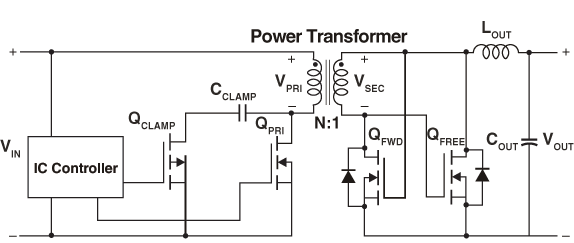
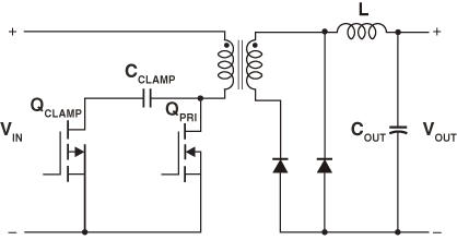
A typical active clamp forward power supply schematic is shown in Figure 1. For the sake of simplicity, just the supply’s power stage and interface to a power supply controller IC are shown. Ancillary components related to the controller IC have been omitted for clarity.

The forward supply’s controller IC operates the two FET switches on the primary side, QPRI and QCLAMP, at a high frequency (100’s of kHz) and in a complementary fashion. When one is on, the other is off. The proportion of the time QPRI is on (QCLAMP is off) during the switching period is referred to as the duty cycle, D. The proportion of time that the primary FET is on results in a pulse train voltage of varying density across the primary of the transformer, VPRI. This voltage waveform is then coupled to the secondary side of the transformer due to the magnetic flux coupling properties of a transformer. The voltage present on the secondary, VSEC, is scaled by the transformer turn’s ratio, N:1.

The secondary voltage pulse train waveform is primarily used to feed the output inductor, LOUT, and capacitor, COUT, through a rectifying circuit, QFWD and QFREE. This low-pass L-C filter is used to filter the pulse train into a DC voltage at the output of the forward power supply, which has a voltage proportional to D and N. The pulse train at VSEC is also often used to drive the FET switches on the secondary side to behave like diodes. This technique is called Synchronous Rectification (SR) and results in better efficiency than using diode rectifiers.
Doc1500-Figure-1-Schematic.gif

Figure 1 -  Active Clamp Forward with Synchronous Rectification

Flyback Operation

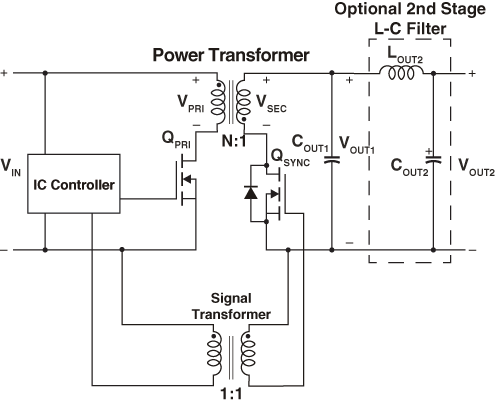
A typical flyback power supply schematic is shown in Figure 2. The flyback supply’s controller IC controls the primary FET switch, QPRI, and the synchronous rectifier, QSYNC, in a complementary fashion. Again, QPRI is modulated at a high frequency with a varying duty cycle, D. Like the forward, the resulting voltage pulse train across the transformer’s primary, VPRI, is coupled onto the transformer’s secondary, VSEC. Unlike the active clamp forward, when QPRI is on, significant energy is stored in the transformer. Then, when QPRI is off (QSYNC is on), this stored energy is released to the secondary.

This means QSYNC is responsible for rectifying the energy of the pulse train present on the secondary. Since a synchronous rectifier is used for QSYNC instead of a simple diode rectifier, the IC controller’s gate drive signal needs to cross the isolation boundary to get to the secondary side FET. A relatively small, simple gate drive signal transformer accomplishes this.
Doc1500-Figure-2-Schematic.gif

Figure 2 - Flyback with Synchronous Rectification

The flyback’s output filtering also differs from the forward supply. For a flyback, the output L-C comprises the primary inductance of the power transformer and the output capacitor, COUT1. The resulting filtered DC output voltage at VOUT1, like the forward, is proportional to D and the power transformer’s turns ratio, N. In addition to this L-C filter, flybacks frequently make use of an optional, second stage L-C filter comprising LOUT2 and COUT2. This optional low-pass filter further attenuates the pulse train’s AC content, reducing the ripple at VOUT2.

Comparing Forward & Flyback Supplies

Parts Count, Output Filtering

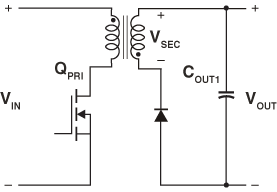
Perhaps the most straightforward comparison to make when debating forward vs. flyback is the parts count between the two topologies, particularly given the implications it has on a power supply’s solution size and total cost. Figure 3 shows a traditional, simple version of a flyback. QSYNC of Figure 2 was replaced with a diode rectifier and the second stage L-C filter was not used.

Doc1500-Figure-3-Schematic.gif

Figure 3 - Simplest Flyback
 

  Forward Flyback
Traditional Modern Modern Traditional
Decreasing
Component
Expense
Power Transformer 1 1 1 1
Controller IC 1 1 1 1
FETs 2 4 2 1
Output Inductor 1 1 1 0
Signal Transformer 0 0 1 0
Rectifier Diodes 2 0 0 1
Output Capacitors 1 1 2 1
TOTAL 8 8 8 5

Table 1 - Parts Count of Forwards and Flybacks

Doc1500-Figure-4-Schematic.gif

Figure 4 - Simplest Forward

Similarly, a simple version of an active clamp forward is shown with diode rectifiers in Figure 4. As seen in Table 1, the flyback is a clear parts-count winner in these traditional implementations. Perhaps this is the source of the “flybacks are simpler and cheaper” rule of thumb.

However, modern implementations of telecom-oriented active clamp forward and continuous conduction flyback power supplies frequently use synchronous rectification as shown in Figures 1 and 2, as well as a two-stage output filter for flyback topologies. As shown in Table 1, this narrows the parts count and complexity gap between the two topologies, rendering the “flybacks are simpler and cheaper” rule of thumb largely moot.

The nearly ubiquitous use of synchronous rectification is due to a couple of primary factors:

  • The steady cost decline of SR capable controller ICs and FETs
  • The lower output voltage and higher output power requirements of today’s power supplies

As one can imagine, attempting to use diode rectification for a 3.3 V output voltage with a 20 A output current requirement would be unacceptable. Rectifying 20 A, even with a Schottky diode, would result in approximately 10 W of loss if the forward voltage drop was 0.5 V. It is difficult to remove this much power from a single device – not to mention the resulting reduction in power supply efficiency. This contrasts with using a synchronously-rectified FET which could easily have a resistance of approximately 2.5 mΩ. In this scenario, the FET would only dissipate about 1W = (20 A)2 X 2.5 mΩ. It is considerably easier to get this amount of power out of a single component. Typically, a large, expensive heatsink would be used to cool the diode versus a moderately-sized Printed Circuit Board (PCB) pad for the FET.

In its simplest form, adding synchronous rectification to a forward requires each power transformer’s secondary terminal to be connected to the synchronous-rectifier FET’s gates as seen in Figure 1. This technique is often called Self-Driven Synchronous Rectification (SDSR). With higher voltage outputs comes higher secondary voltages. Because of this, a level translator or clamp circuit may be required to keep the gate drive voltage within the FET’s absolute maximum ratings. Since these circuits are relatively small and use inexpensive components, they are not accounted for in Table 1.

For esoteric reasons, continuous conduction SR flybacks do not work well with SDSR, unlike the active clamp forward. As mentioned previously, the consequence for using SR for a continuous conduction flyback is the need for a signal transformer to get the gate drive signal across the isolation boundary. Using Coilcraft’s new LPD8035V Series of miniature 1500 Vrms isolation transformers makes adding this component relatively painless due to its small size and low cost.

Another reason for the narrowing of the component count between the two modern power supply topologies is the addition of the second stage of a two-stage L-C filter for flybacks. It is often said that flybacks are more electrically noisy than forwards due to the larger ripple current in their secondaries. This means if you are using a single-stage L-C filter for a flyback, a much larger inductor and capacitor would be required to keep the output ripple the same as a forward. In practice, several methods can be employed to achieve comparable output ripple from a flyback:

  • A larger power transformer with its commensurate larger inductance
  • A larger output capacitor
  • A two-stage L-C filter
doc1500_figure5.jpg

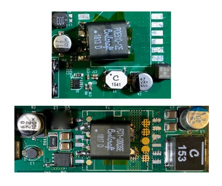
Figure 5 – Flyback (top) and Forward (bottom) Examples

The first two filtering options usually result in a larger, more expensive solution. By using a two-stage L-C filter, each of the two inductors and two capacitors can be selected to optimize a specific attribute (low ripple current, low core loss, etc.) This almost always leads to a smaller-sized and less expensive overall filter design to achieve the same ripple voltage.

For the reasons outlined, the component count, solution size, and overall solution cost for the forward and flyback are closer than they have traditionally been. Table 2 shows the results of an empirical size and cost comparison between forward and flyback power supply designs. These designs are both 12 V output, 51 W supplies based on Analog Devices’ LT4295 PD Controller IC. Physical pictures of the two PCBs are shown in Figure 5 and the simplified schematics are shown in Figures 1 and 2. As can be seen from Table 2, the flyback remains smaller and less expensive, but not dramatically so.

  Forward Flyback
Size (in2) 3.2 2.6
Cost (normalized) 100% 90%
Efficiency (at 4 AOUT) 94.3% 92.8%
FET stress, pri (max) 90 V 146 V
FET stress, sec (max) 85 V 126 V
 
Table 2 - Forward and Flyback Comparison Summary  

Efficiency

Another perception is that forward power supplies are much more efficient than flyback supplies. This was likely true in the past. This can be attributed to the simplest forward power supply having twice as many FETs, diodes, and magnetic components (transformers and inductors) as seen in Figures 3 and 4. With double the components, it is easier to optimize each component’s attributes and spread out the power dissipation across multiple components.

For example, a flyback’s transformer does double duty to implement galvanic isolation and the inductance used for L-C filtering. This contrasts with the forward that has a separate transformer for isolation and a separate inductor for filtering: each component is selected to perform a single purpose.

This usually leads to choosing lower resistance inductors and smaller transformer cores to minimize losses within the forward supply.

Another example is the forward’s use of multiple semiconductors compared to one for the flyback. This is shown in Figures 3 and 4 where the active clamp forward uses two FET switches in the primary versus one in the flyback. Likewise, two diode rectifiers were traditionally used in the forward and one diode for the flyback. This puts the flyback at a disadvantage; all the secondary currents had to be processed by a single rectifier diode and all the primary currents with a single FET. With the higher costs and lower performance of semiconductors in the past, this often led power supply designers to skimp on the size of the larger, more expensive flyback semiconductors. This led to higher power dissipations, and thus lower flyback efficiencies.

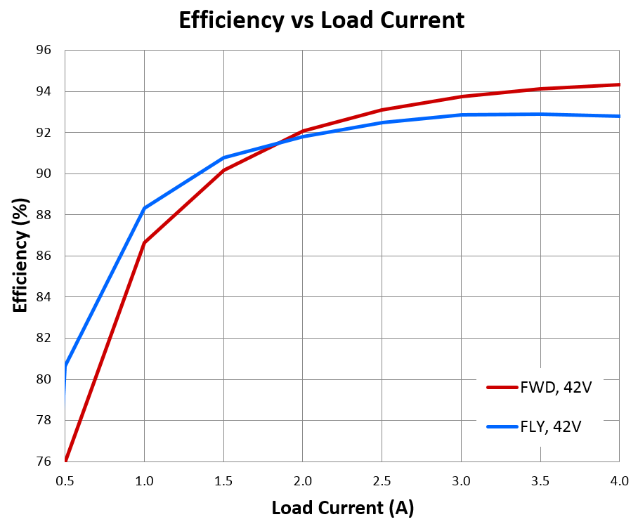
The use of modern techniques and components has narrowed the efficiency gap between the two power supply topologies quite a bit. For example, moving to synchronous rectification with modern FETs has considerably reduced rectifier losses as a percentage of a power supply’s total losses. As FETs have improved over the decades, even the primary FETs contribute a smaller percentage of efficiency loss. An increase in the number of transformer core geometries and materials available has resulted in much smaller, efficient and more cost-effective flyback transformers. An example of these new transformer cores is seen in the new line of Coilcraft POE51Q-12E flyback and FCT1-120Q3SE forward transformers geared to the new IEEE 802.3bt standard. The results of all these factors can be seen in comparing the narrow 1.5% efficiency gap at a load of 4 A on the output of the example power supplies in Table 2. Figure 6 shows the efficiency curves for the forward and flyback example circuit over the entire load current range.

Doc1500-Figure-6.png

Figure 6 - Effieciency over Load Current

FET Voltage Stresses

FET voltage stresses for active clamp forward and most flyback power supplies tend to favor the forward. This is a consequence of a couple of factors, the first being transformer leakage inductance.

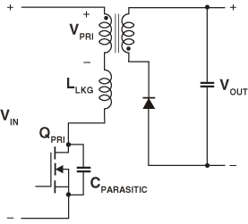
Leakage inductance is a result of imperfect coupling, or linking, between the primary and secondary windings which allows magnetic flux to “leak out” between the two windings. Larger transformers tend to have a larger area for this flux leakage to occur. For a given power output, flyback transformers tend to be larger than their forward counterparts, resulting in higher leakage inductance.

Doc1500-Figure-7-Schematic.gif

Figure 7 - Leakage Inductance of a Flyback

Leakage inductance is typically modeled as a separate inductance, LLKG in series with the primary winding as seen in Figure #7. When the primary FET turns off, the current that was flowing in LLKG needs to be maintained. This leakage current is dumped into the relatively small parasitic capacitance, CPARASITIC, on the FET’s drain node which causes a fast, resonant spike due to the L-C circuit as seen in Figure #8. This spike on the drain nodes results in a higher required FET voltage rating.

Doc1500-Figure-7-Flyback-FET-Stress-(RAW).jpg

Figure 8 - Leakage Spike of a Flyback

The way the active clamp forward handles the transformer leakage inductance stands in contrast to the flyback. The forward topology makes use of a clamp capacitor, CCLAMP, and a clamp FET, QCLAMP, as seen in Figure 1. When the primary FET, QPRI, turns off, the leakage current is now steered into CCLAMP by the QCLAMP FET. CCLAMP is a controlled capacitance value that is much larger than the parasitic capacitance on the drain node of the flyback’s QPRI. With a properly sized CCLAMP and proper control of QCLAMP, virtually no spiking occurs on the active clamp forward as seen in Figure 9. Table 2 summarizes the max voltage spike for the two topologies’ maximum FET stresses.

Doc1500-Figure-8-Forward-FET-Stress-(RAW).jpg

Figure 9 - Leakage Spike of a Forward

The flyback’s larger transformer and the leakage clamping behavior of the active clamp forward are the reasons the FET drain voltage level is lower in the forward. This fact allows for a lower voltage rating FET to be selected. Since the FET’s channel resistance, RDS(ON), is exponentially and inversely proportional to the rated voltage, the forward, again, gets a slight efficiency edge. In Figure 10, the resultant lower temperature of the forward’s QPRI can clearly be seen.

Doc1500-Figure9-FWD-vs-FLY,-bottom-(RAW).jpg Doc1500-Figure9-FWD-vs-FLY,-top-(RAW).jpg
Figure 10 - Thermographs of the Forward/Flyback Examples

The leakage spike illustrates one of the obvious shortcomings of a flyback supply. Given its importance to the success of an isolated power supply, this is one of many reasons that having a good transformer design should be left to the experts. The designers at Coilcraft understand all the trade-offs of modern forward and flyback transformer design. In addition to decades of custom design support, Coilcraft’s broad manufacturing footprint also assures product quality, availability and competitive pricing.

Revised Rules of Thumb

Despite several of the traditionally held rules of thumb being called into question, some generalizations can still be made between modern active clamp forward and continuous flyback power supplies, at least in the telecom input voltage range.

Modern forward supplies tend to be more efficient. The first reason is the active clamp behavior of the forward’s primary FET results in the need for lower voltage rating, lower RDS(on) FETs. Another reason is the doubling of the power stage components used in the forward. In the case of the forward’s magnetics, this allows the designer to optimize two individual components instead of being locked into using one component. Figure 10 shows that the two forward magnetics run cooler than the flyback’s single transformer. In the case of the FETs in a forward supply, distributing the power losses over two components versus one decreases the individual component losses which increases efficiency. This is especially helpful in increasing the forward’s efficiency for high current, low output voltage supplies. Splitting up a flyback’s single synchronous rectifier FET into two FETs in the forward allows for more current to be processed more efficiently.

While having a larger number of power stage components helps increase the forward’s efficiency, the component’s relatively high cost tends to make forward power supplies marginally more expensive. Another result of the higher number of relatively large components is the forward has a somewhat larger PCB footprint.

So, Which is Better?

The discussions in this article should make it clear that forward and flyback power supplies have unique characteristics that make each suitable for optimizing different requirements: cost, size, and efficiency. Boiling down all the above attributes, one could argue that flybacks should still be considered the default choice for most power supply requirements due to their somewhat smaller size, lower cost, and comparably high efficiency. When the supply requirement exists for the absolute best in efficiency, the forward topology should be considered first. So, which is better?

Both!

Doc 1500

Questions or Concerns?

Ask View FAQs


General Applications

Handling and Processing

RF Inductors

Power Conversion

EMI/RFI Filtering

Special Applications