Noise limits set by regulatory agencies make solutions to common mode EMI a necessary consideration in the manufacture and use of electronic equipment. Common mode filters are generally relied upon to suppress line conducted common mode interference. When properly designed, these filters successfully and reliably reduce common mode noise. However, successful design of common mode filters requires foresight into the nonideal character of filter components — the inductor in particular. It is the aim of this paper to provide filter designers the knowledge required to identify those characteristics critical to desired filter performance.
The filtering of common mode noise is typically not as well understood as its differential counterpart and this paper deals with the practical aspects of common mode filters as related specifically to the common mode inductor. Common mode noise occurs simultaneously on both lines of a conductor pair with respect to a common ground, whereas differential noise occurs between conductor paths. The frequency response characteristics of filters incorporating different common mode choke constructions is examined. The filter designer should then have a better understanding of common mode inductors and be able to choose the common mode inductor construction which will yield the required attenuation characteristic without the additional cost of over-designing or the failure of under-designing the component.
Power converters are often major sources of noise in any equipment. Power converters normally produce common mode and differential mode noise at harmonics of the switching frequency while some wide band differential mode noise is usually also produced. 1
Conducted emissions from power converters are attributable to a number of causes. The nature of converter operation (the rectification of the line frequency, and switching waveforms, for example) and circuit magnetics contribute several unique types of noise; also, the capacitive effects of components and overall mechanical structures, such as cases, and the semiconductor components themselves add their own disruptive voltages. An input L-C smoothing filter is generally required in off-line switching regulators, but these inductors and capacitors may themselves be sources of EMI. If the inductor is constructed with a relatively high Q material, it will display substantial ringing and produce spectral noise energy. Also, switching noise of the converter may be coupled back into the line through the distributed capacitance of the inductor. The power transformer may also ring and couple in ways similar to the filter inductor and produce its own EMI.
There are semiconductor noise sources associated with temperature (thermal noise) within the junction of differing materials (contact noise) and electron-hole movement in junction devices (shot noise). There exists low frequency noise attributable to dc current carrying electronic devices (modulation, flicker, or 1/f noise), due to the non-ohmic behavior of semiconductors at high fields (hot carrier noise), the generation and recombination of charge carriers (generation-recombination noise), and inducted noise at the gate of an FET due to the alteration of the source to drain currents by the induced charge at the gate. 2
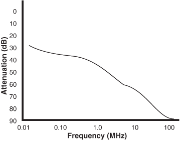
Figure 1. Ideal frequency response predicted for second order filter with Coilcraft E3493 common mode inductor and 0.005 µF capacitors.
Real filters do not follow the theoretical expectations provided by standard filter alignments (Bessel, Chebyschev and Butterworth — See Appendix A). For example the expected frequency response of a typical second order low pass filter is shown in Figure 1. However, due to the self-resonant behavior of common mode inductors (and any inductor), the observed response is actually similar to that shown in Figure 2.
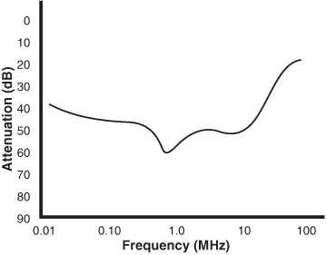
Figure 2. Measured frequency response of second order filter with Coilcraft E3493 common mode inductor and 0.005 µF capacitors.
At frequencies below resonance, where the filter components are nearly ideal, standard filter configurations yield very nearly theoretical results. Inductors, ideally, provide an impedance which is directly proportional to frequency, but this is only true for a long, single layer aircore cylindrically wound coil with large gauge wire (i.e., the ‘perfect’ coil).
At frequencies above self-resonance, an inductor begins to display the full effects of its parasitic components, particularly the distributed capacitance (Cd).
The Cd describes the effective capacity across an inductor and is caused by individual turns of wire in close proximity (Figure 3). It is the distributed capacitance that gives the inductor its characteristic self-resonant frequency (1 ⁄ 2π√LC ).
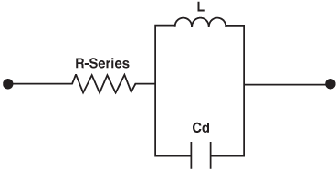
Figure 3. Model of an inductor (one common mode inductor winding).
Other non-ideal aspects of inductors include leakage inductance, which acts as inductance in series with each winding. All multiple winding chokes display leakage inductance. The leakage inductance of a winding is the amount of inductance which is not coupled to any other windings through a shared core and is undesirable in transformers because it stores energy without transforming it to other windings in the structure. In a low pass filter, however, leakage inductance adds to the attenuation of the filter. In line frequency common mode chokes (i.e. where the differential signal passes unattenuated due to coupling of the winds) the uncoupled leakage inductance will aid in the suppression of high frequency differential noise.
Resistive losses such as copper (I2R) and core loss also affect attenuation. The diameter of wire used in a choke is determined by the amount of current which it will be required to handle. The larger the current, the larger the wire. For example, at a line frequency current of 1 Ampere, 26 AWG wire is required to provide 250 circular mils to support the current. As frequency increases, the amount of cross sectional area (for a single strand of wire) used by the current decreases (skin effect). For frequencies above about 100 kHz, multistranded wire (litz wire, with each strand insulated) should be used if the high frequency current is to be supported. For a low pass inductive filter that needs to pass only the line frequencies, further attenuation due to skin effect is actually desirable.
Capacitors exhibit parasitics of their own. For filter applications, mylar, mica, and ceramic capacitors are the most useful because they exhibit high self-resonant frequencies due to minimization of their parasitics (series inductance and resistance, and parallel resistance).
Three winding configurations for inductors are shown in Figure 4. The most simple and least prone to distributed capacitance of all the standard configurations is the single layer wind. The starts and finishes of a single layer wind are as far from one another as possible, thus reducing capacitive coupling. A multilayer wind (two or more single layers) provides capacitance between layers as well as from the start lead to the finish lead (that are generally close to one another with the finish lead ending where the start lead began). The multilayer configuration displays the greatest capacitance of the winding configurations (thus the lowest attenuation at higher frequencies for an inductive low pass filter).

Figure 4. The three winding configurations examined
A compromise between the single and multi-layer winding configurations is the third configuration: the progressive (banked) wind. A progressive wind is accomplished by winding a few turns, then backing up a couple of turns and repeating the process (‘three steps forward and two steps back’). The start and finish leads are thus as far apart as possible, with the same number of turns as a multilayer wind, but without the interleaving. The distributed capacitance of a progressive winding configuration is between that of a single layer wind and a multilayer wind.
In general, above the self-resonant frequency, chokes become largely dissipative, yielding roughly constant and substantial resistance for a very limited frequency band (a few octaves at most); above this limited band, the chokes become predominately capacitive (Figure 5).

Figure 5. Typical inductor impedance characteristic (Coilcraft E3490).
The self-resonant frequency of a filter’s inductor determines the resonant frequency of the filter itself; maximum attenuation is normally achieved near this frequency
The capacitor (in a second order filter configuration) determines the attenuating behavior of the filter at frequencies above resonance (Figure 6), and with very little capacitance, the filter response exhibits the rapid decrease of attenuation due to the inductor response. A larger value capacitor will increase the slope of attenuation after resonance for a limited band of frequencies. A very large filter capacitor, used to maintain stability out to high frequencies, will cause the post resonant attenuation to increase over that achieved at resonance.

Figure 6. Frequency response of a 2nd order filter with Coilcraft E3495 for various capacitor values.
Table 1 shows the electrical characteristics of one wind of each of the common mode chokes.
| Part | L@10kHz (mH) | Freq (MHz) |
|---|---|---|
| E3499 | 20.70 | 0.2 to 0.3 |
| G6252 | 17.70 | 0.2 to 0.3 |
| E3490 | 10.90 | 0.3 to 0.4 |
| E5705 | 6.44 | 0.5 to 1.0 |
| P104 | 4.00 | 0.5 to 1.0 |
| E3493 | 3.30 | 0.5 to 1.0 |
| A-S | 2.60 | 1.0 to 2.0 |
| A-P | 2.50 | 1.0 to 2.0 |
| F5806 | 1.70 | 1.0 to 2.0 |
| F5593 | 1.50 | 0.5 to 1.0 |
| B-S | 1.20 | 1.0 to 2.0 |
| B-P | 1.20 | 1.0 to 2.0 |
| B-D | 1.20 | 1.0 to 2.0 |
| F3495 | 1.08 | 1.0 to 2.0 |
| C-D | 0.85 | 0.5 to 1.0 |
| C-P | 0.84 | 1.0 to 2.0 |
| C-S | 0.80 | 1.0 to 2.0 |
| E3506 | 0.71 | 1.0 to 2.0 |
| D-D | 0.27 | 2.5 |
| D-S | 0.27 | 4.0 |
| E-S | 0.26 | 5.0 to 6.0 |
| E-D | 0.23 | 3.0 to 4.0 |
| E-P | 0.21 | 5.0 to 6.0 |
Table 1. Self-resonant frequency ranges and initial inductance values for the common mode chokes examined. Note the change in resonant frequency of the double layer (-D) compared to the equivalently constructed single layer (‑S) and progressively wound (-P) chokes.
For similar constructions, self-resonance (the useful and theoretically predictable frequency limit of inductance) generally decreases as initial inductance (measured between 10 kHz and 20 kHz) increases. Moreover, the self-resonant frequency of a layer wound inductor decreases as the number of layers are increased (while maintaining the same turn count).
The progressive or banked windings (-P) of the table display the same self-resonance as the single layer (-S) versions. Progressive winding allows the increased turns of a multilayer wind while maintaining the optimum characteristics of a single layer wind.
Because our examination was to determine the attenuation effected by a typical EMI filter configuration due to differing chokes and choke constructions, we used the circuit shown in Figure 7, maintaining all circuit components constant except for the inductive element.

Figure 7. Test circuit used to measure common mode signal attenuation.
We initially felt it necessary to determine whether differential power (60 Hz) applied to the common mode circuit would affect the high frequency common mode attenuation of the filter. Presumably, the differential operation of the common mode circuit, with inductors coupled to each other and their relative polarity such that their equal and opposite (differentially produced) flux lines cancel, no inductive reactance should be encountered by the differential signal and saturation of the core should therefore not occur from the differential signal. To prove this we used the circuit shown in Figure 8 with a load, RL, to provide the rated current through the choke.

Figure 8. Test circuit used to apply common mode signal and differential (60 Hz) power simultaneously
The LISN (see Appendix B) of the “power” circuit was split at 2 MHz between the standard 50 µHenry/5 Ohm arrangement (below 2 MHz) and the 50 µFarad/50 Ohm arrangement (providing 50 Ohms above 2 MHz to the noise source). Splitting the LISN (and later splicing the attenuation curves at 2 MHz) provided a more accurate composite LISN than either arrangement alone would have with the required power components.
Neglecting measurement error (approximately 4 decibels), the differential input did not appear to affect the common mode attenuation of the circuit even at high frequencies (through 10 MHz).
Figures 9 and 10 show the common mode attenuation by second order filters with the standard chokes and 0.005 µF capacitors and using the LISN load.

Figure 9. Common mode attenuation of second order filters with 0.005 µF capacitors and various toroid inductors.

Figure 10. Common mode attenuation of second order filters with 0.005 µF capacitors and various E core inductors.
The attenuation plots vary greatly below 10 MHz and above 70 MHz, but provide very similar attenuation between these frequencies. Above 10 MHz, the capacitor and its anomalies dominate the filter’s attenuation, and above 70 MHz the distributed capacitance of the choke shunts increasingly more noise signal across the choke as frequency increases. If the distributed capacitance of a choke is increased (e.g., by multi-layer) the filter attenuation further decreases and displays this decrease at lower frequencies.
Figures 11 and 12 display the effect of increased distributed capacity (by double layering) of various chokes and constructions.

Figure 11. The effect on attenuation due to the differing distributed capacitance of single and double layered winds.

Figure 12. The effect on attenuation due to the differing distributed capacitance of single and double layered winds.
When comparing the attenuation data of the three configurations (S=single layer; P=progressive wind; D=double layer), the difference between the single and progressive wound chokes are not very significant; the double layer versions do, however, display less attenuation at high frequencies than either the progressive or single layer chokes.
Figure 13 shows the effect of leakage inductance on attenuation. It was expected that increased leakage inductance may slightly increase the high frequency common mode attenuation. From the data taken, however, no such trend was apparent, and it appears that typical changes in the leakage inductance do not significantly affect the performance of common mode inductors.

Figure 13. The effect on attenuation due to leakage inductance.
The data taken can be used in the following ways:
Common mode filter response differs substantially from theoretically predicted performance. Filter performance can be explained and successfully manipulated if nonideal component response is taken into account. The common mode inductor is a primary component in determining the response of a typical filter circuit. The common mode inductor affects the magnitude (maximum attainable attenuation) and the shape (resonant frequency) of the frequency response of the filter.
A filter designer should carefully consider filter response from approximately 1 MHz to 30 MHz to determine whether the slightly diminished attenuation of a multiple layer inductor is acceptable. If one were to specify the inductor to be single layer it may result in unnecessary cost and size penalties. The winding pattern of the individual windings (Cd) is far more significant than the relationship of the two windings (leakage inductance).
The distributed capacitance of a choke decreases attenuation at high frequencies and multilayering increases the distributed capacitance of an inductor. Progressive winding allows the equivalent number of turns of wire as a multilayer and usually far more turns than a single layer could accommodate. A progressively wound inductor will display a distributed capacitance similar to a single layer. To attenuate noise voltages which occur above the limits prescribed by the FCC and VDE, the filter designer may opt for the progressively wound inductor.
Passive filters serve as a very good means of eliminating the majority of conducted noise into a device (or out of a device and back into the line) when relatively high current is flowing. Many filter configurations exist and each has its own advantages. Commonly considered filter alignments are the Chebyshev, the Butterworth, and the Bessel.
The ideal Chebyshev low pass filter alignments allow a compromise between the amount of ripple in the passband (and damping) and the slope of attenuation at the cutoff frequency. The stable behavior of the time response of Chebyschev filters is related to the damping factor, the allowed ripple, and the slope of attenuation at the cutoff frequency; as the slope of the attenuation at the cutoff is increased, the transient response becomes less stable and prone to ringing, and the phase response becomes much less linear.
Butterworth low pass filter alignments are Chebyshev filters designed for minimum ripple and ideally provide a flat response, no attenuation prior to the cutoff frequency, and a damping factor of approximately 0.7. After the cutoff frequency, the attenuation begins and continues at 20 times the order in decibels per decade. The time response for the Butterworth filter exhibits some ringing and the phase response is not ideal, but predictable. The overall response of Butterworth filters is well suited to quick and easy methods of approximation. Ideally, Bessel filters maintain a very stable, linear phase response but at the expense of frequency response; the time response of Bessel filters is well behaved without substantial overshoot or ringing.
In their use as noise suppressors, filters must be able to eliminate as much noise as possible over a predetermined frequency band. As long as the inherent ringing of the filter is low (does not itself become a noise source) it is the frequency rather than the time response of a filter that is an important concern. In a common mode filter, the differential signal does not encounter the filter, thus any problems associated with phase or time response affect only the common mode noise. When the filter is used to keep noise from entering the power mains from the device, phase and time responses become trivial to even the differential voltage.
Butterworth alignments for the design of EMI filters are an appropriate starting point; they are easily modeled, readily approximated and constructed, and provide good frequency response with relatively little ringing.
A major object of testing a component part or device is the ability to repeat the testing with the same results regardless of the time or place of the test. When testing requires the power line to be stable, or at least standard for a test, adjustments must usually be made or spurious results may occur.
Power lines may vary in output impedance by as much as 40 Ohms from location to location, making the repeatability of line based evaluations very unreliable between differing locations. A Line Impedance Stabilizing Network (LISN, or Artificial Mains Network: AMN) allows uniform line based testing regardless of locality. A line impedance standard has been devised and is specified by several licensing and independent safety agencies (e.g., the FCC and VDE; see Figure 14). 3

Figure 14. LISN characteristic specified by FCC Docket 20780 and VDE 0876 Part 1.
(1) Schneider, Len M. “Noise Sources Equivalent Circuit Model for Off-Line Converters and Its use in Input Filter Design.” Proceedings of Powercon 10, March 1983, P. C-1.
(2) Scidmore, A.K. “Noise in Amplifiers.” Lecture Notes for ECE-341—Linear Active Circuits, University of Wisconsin: 1982.
(3) Nave, Mark “Line Impedance Stabilizing Networks: Theory and Use.” RF Design,April 1985, P. 54.
Kendall, C.M. and Schmid, A.A. “Characteristics and Control of EMI in a Switching Regulator Power Converter.” Proceedings of Powercon 10, March 1983, P. C-4.
Head, Mike “Know RF-Emission Regulations Pertaining to Your Design.” EDN, August 1981.
Kociecki, John “Predicting the Performance of CommonMode Inductors.” Powerconversion International, March 1984, P. 56.
Carsten, Bruce W. “Design Techniques for the Inherent Reduction of Power Converter EMI.” Proceedings of Powercon 11, March 1984, P. D-2.
Nye, J.F. Physical Properties of Crystals. Oxford University Press, 1972.
Williams, Arthur B. Electronic Filter Design Handbook. McGraw-Hill, 1981.